What is a Half Adder?
A Half Adder is a combinational logic circuit that performs binary addition of two single-bit inputs:
- Input A
- Input B
It produces two outputs:
- Sum: A XOR B
- Carry: A AND B
Unlike a Full Adder, it does not handle carry input from a previous stage, which limits its use to the simplest addition operations.
Truth Table of Half Adder
|
Input A |
Input B |
Sum (A ⊕ B) |
Carry (A · B) |
|
0 |
0 |
0 |
0 |
|
0 |
1 |
1 |
0 |
|
1 |
0 |
1 |
0 |
|
1 |
1 |
0 |
1 |
Verilog Code for Half Adder
Module: Half Adder
// Pantech e-learning
// Half adder implementation using structural modelling
module half_adder(
input a,
input b,
output sum,
output cout);
xor (sum, a, b);
and (cout, a, b);
endmodule
Testbench for Half Adder
// Pantech e-learning
module half_adder_tb;
reg a, b;
wire sum, cout;
half_adder uut(
.a(a), .b(b), .sum(sum), .cout(cout)
);
initial begin
$dumpfile(“dump.vcd”);
$dumpvars(0, half_adder_tb);
a = 1’b0; b = 1’b0;
#10 a = 1’b0; b = 1’b1;
#10 a = 1’b1; b = 1’b0;
#10 a = 1’b1; b = 1’b1;
#10;
end
endmodule
Waveform Output
After running the simulation, you will observe the correct generation of Sum and Carry outputs for all binary input combinations. Use waveform viewers like GTKWave to analyze the output transitions clearly.

Figure: Half Adder simulation waveform output
Frequently Asked Questions (FAQs)
Q1: What is the main purpose of a Half Adder?
A Half Adder is used to add two single-bit binary numbers and generate a sum and carry.
Q2: Why is it called a “Half” Adder?
Because it only adds two inputs and does not process a carry-in from a previous stage.
Q3: What logic gates are used in a Half Adder?
It uses an XOR gate for the sum and an AND gate for the carry.
Q4: What happens when both inputs A and B are 1?
The Sum output is 0, and the Carry output is 1.
Q5: Can a Half Adder be used for multi-bit addition?
Not directly. For multi-bit addition, Full Adders are used as they include a carry-in input.
Conclusion
In this blog, you learned the working principle of a Half Adder and how to implement and simulate it using Verilog. Understanding this basic building block is essential before moving on to Full Adders and complex arithmetic circuits.
Call to Action
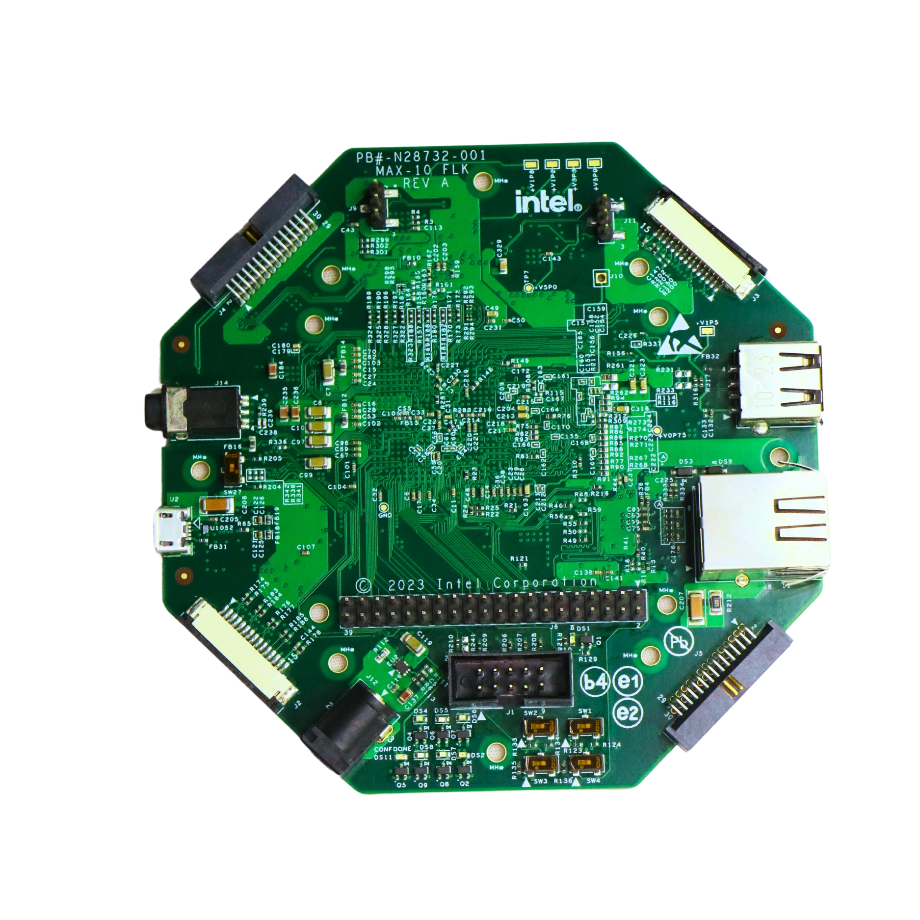
Try implementing this Half Adder on a MAX10 FLK FPGA board and observe the Sum and Carry outputs live.
Want to go deeper into digital logic design? Explore Pantech’s complete Verilog series and join our hands-on internship program to master FPGA development from scratch!
- All Projects
- Product