What is a Full Adder?
A Full Adder is a combinational logic circuit that adds three one-bit binary inputs:
- A (first input)
- B (second input)
- Cin (carry-in from the previous stage)
It produces two outputs:
- Sum: the result of the binary addition
- Cout: the carry-out to the next adder stage
This makes the Full Adder suitable for cascading in multi-bit adder circuits like Ripple Carry Adders.
Truth Table of Full Adder
|
A |
B |
Cin |
Sum |
Cout |
|
0 |
0 |
0 |
0 |
0 |
|
0 |
0 |
1 |
1 |
0 |
|
0 |
1 |
0 |
1 |
0 |
|
0 |
1 |
1 |
0 |
1 |
|
1 |
0 |
0 |
1 |
0 |
|
1 |
0 |
1 |
0 |
1 |
|
1 |
1 |
0 |
0 |
1 |
|
1 |
1 |
1 |
1 |
1 |
Verilog Code for Full Adder
Design
// Pantech e-learning
// Full adder implementation using structural modelling
module full_adder(
input a,
input b,
input c,
output sum,
output cout);
wire w1, w2, w3;
xor (w1, a, b);
xor (sum, w1, c);
and (w2, c, w1);
and (w3, a, b);
or (cout, w2, w3);
endmodule
Testbench
// Pantech e-learning
module full_adder_tb;
reg a, b, c;
wire sum, cout;
full_adder uut (
.a(a), .b(b), .c(c), .sum(sum), .cout(cout)
);
initial begin
$dumpfile(“dump.vcd”);
$dumpvars(0, full_adder_tb);
a = 1’b0; b = 1’b0; c = 1’b0;
#10 a = 1’b0; b = 1’b0; c = 1’b1;
#10 a = 1’b0; b = 1’b1; c = 1’b0;
#10 a = 1’b0; b = 1’b1; c = 1’b1;
#10 a = 1’b1; b = 1’b0; c = 1’b0;
#10 a = 1’b1; b = 1’b0; c = 1’b1;
#10 a = 1’b1; b = 1’b1; c = 1’b0;
#10 a = 1’b1; b = 1’b1; c = 1’b1;
#10;
end
endmodule
Output
You can visualize the waveform using GTKWave. The simulation will show the sum and cout for all possible combinations of inputs A, B, and Cin.

Figure: Full adder simulation output
Applications
- Used as the fundamental building block for Ripple Carry Adders
- Part of ALUs in processors
- Employed in arithmetic operations in FPGAs and ASICs
Frequently Asked Questions (FAQs)
Q1: What is the difference between a Half Adder and a Full Adder?
A Half Adder adds two inputs, while a Full Adder adds three inputs including a carry-in, making it suitable for multi-bit binary addition.
Q2: Why is a Full Adder important in digital electronics?
A Full Adder is essential for performing binary addition in multi-bit operations, making it a core building block in ALUs and processors.
Q3: What logic gates are used in a Full Adder?
A Full Adder typically uses XOR, AND, and OR gates. It can also be implemented using two Half Adders and one OR gate.
Q4: What is the expression for the Sum output in a Full Adder?
Sum = A ⊕ B ⊕ Cin (XOR of all three input bits)
Q5: Can Full Adders be connected to build multi-bit adders?
Yes, multiple Full Adders can be connected in series to form multi-bit adders like Ripple Carry Adders.
Conclusion
We successfully implemented and simulated a Full Adder using structural modelling in Verilog. This fundamental circuit is key to performing binary addition and is widely used in digital systems and FPGA designs.
Call to Action
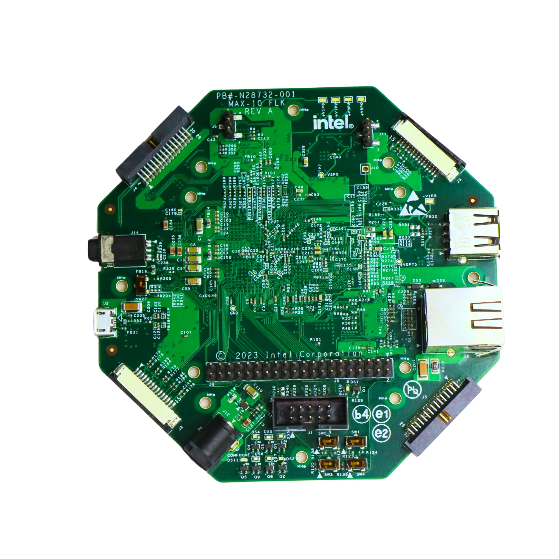
Try building this Full Adder on the Intel MAX10 FLK FPGA board and visualize the simulation results in real-time.
Want to build a complete multi-bit adder? Explore our beginner-friendly Verilog series at Pantech eLearning.
Looking for hands-on training? Join our FPGA/VLSI Internship Program and take your digital design skills to the next level!
- All Projects
- Product