3-Bit Synchronous Counter Using Verilog – Complete Design and Simulation
Description
Build and simulate a 3-bit synchronous counter in Verilog using flip-flops and logic. Step-by-step guide with testbench and waveform.
Introduction
A counter is a basic yet powerful digital component used in most electronic systems. In this blog, we’ll design a 3-bit synchronous counter using Verilog by implementing JK flip-flops with combinational logic. The design and simulation are done using EDAPlayground, making it easy for students and hobbyists to replicate. This is ideal for VLSI labs, digital logic classes, or as a beginner-level project in hardware design.
Core Sections
Understanding the Concept
A synchronous counter uses flip-flops that share a common clock. Each stage toggles based on the logic of the previous stages. In a 3-bit counter, we count from 000 to 111 and then roll over.
Instead of using behavioral-style counter logic (q <= q + 1), this design uses explicit JK flip-flops connected to control toggling at each stage. This helps learners understand how counters work at the gate/flip-flop level.
Verilog Code Explanation
Design
//Pantech e-learning
//Synchronous 3 bit counter using jk flip flop
module jk_ff(
input clk,rst,j,k,
output reg q,q_);
always @(posedge clk) begin
if(rst)begin
q<=0;
end
else if(j == 0 && k == 0)begin
q<=q;
end
else if(j == 0 && k == 1)begin
q<=0;
end
else if(j == 1 && k == 0)begin
q<=1;
end
else if(j == 1 && k == 1)begin
q<=~q;
end
end
assign q_ = ~q;
endmodule
module counter(
input clk,rst,
output[2:0] q,q_);
wire w1 = q[1] & q[0];
jk_ff u1(.clk(clk), .rst(rst), .j(1’b1), .k(1’b1), .q(q[0]), .q_(q_[0]));
jk_ff u2(.clk(clk), .rst(rst), .j(q[0]), .k(q[0]), .q(q[1]), .q_(q_[1]));
jk_ff u3(.clk(clk), .rst(rst), .j(w1), .k(w1), .q(q[2]), .q_(q_[2]));
endmodule
Testbench
//Pantech e-learning
module tb;
reg clk,rst;
wire [2:0] q,q_;
counter uut(.*);
always #5 clk = ~clk;
initial begin
$dumpfile(“waveform.vcd”);
$dumpvars(0,tb);
clk = 0; rst = 1;
#12 rst = 0;
#100;
$finish;
end
always @(posedge clk) begin
$display(“Time = %t, q= %b, q_ = %b”, $time, q,q_);
end
endmodule
Output
Figure 1: Synchronous 3-bit counter using JK flip flop log file
Figure 2: Synchronous 3-bit counter using JK flip flop waveform output
Applications
- Used in digital timers and clocks
- Base design for binary up-counters in processors
- FSM state counters
- Dividers and time delays
- Address generation in memory controllers
FAQs
- Why use JK flip-flops instead of behavioral q + 1?
Using JK flip-flops helps students visualize how hardware is built using fundamental flip-flops and logic. It’s closer to how things are implemented at the gate level. - What happens when reset is applied?
All flip-flops are reset to 0 synchronously on the next clock edge. - Can we design a down counter similarly?
Yes, with appropriate toggling logic adjustments or by subtracting the counter output. - Why is j0 and k0 always 1?
It ensures the first flip-flop toggles on every clock, driving the others based on its output. - Is this design synthesizable?
Yes. This flip-flop-based structure is synthesizable for FPGA or ASIC implementation.
Conclusion
This blog walked you through creating a 3-bit synchronous counter using T flip-flops in Verilog. You learned how to structure logic for toggling, simulate it, and understand real-time waveform behavior. It’s a great stepping stone to deeper sequential logic design.
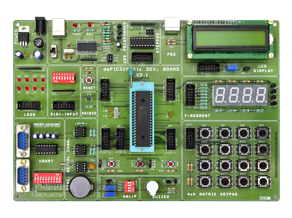
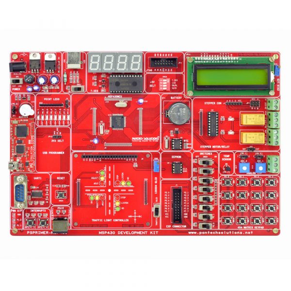
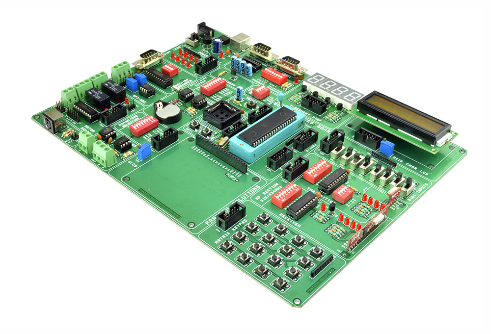
Try this in your VLSI Lab using our trainer kit!
Optional Add-ons
About Author:
A. Manikandan is an RTL Engineer at Pantech India Solutions Pvt. Ltd. With a strong passion for digital design ,FPGAs and ASIC bus protocols. he specializes in FPGA and hardware development, sharing insights to bridge the gap between academia and industry.
You can adjust the second line to reflect any specific expertise or areas of interest you wish to highlight!
Looking Ahead: Collaborate With Us
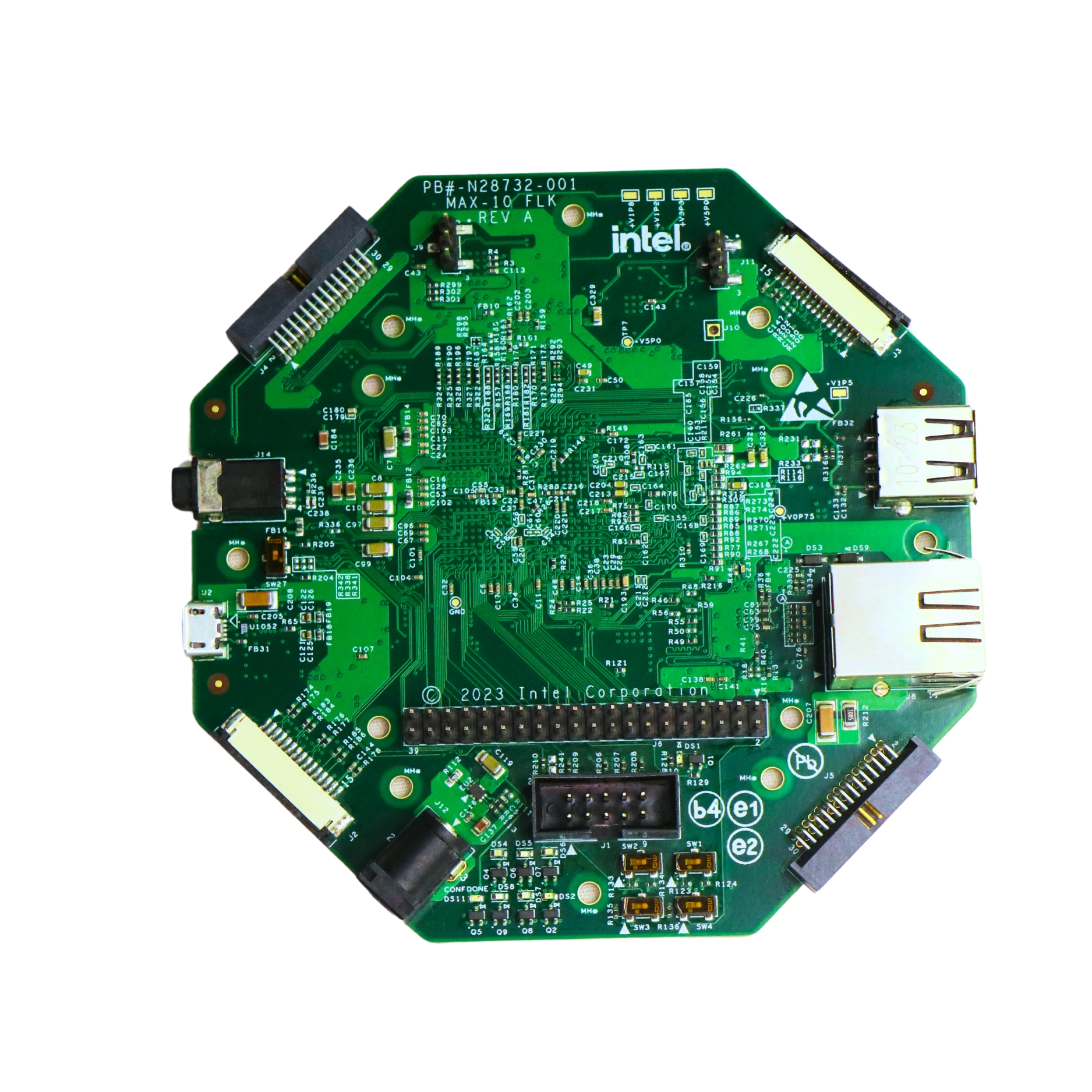
- Try building this Full Adder on the Intel MAX10 FLK FPGA board and visualize the simulation results in real-time.
- Want to build a complete multi-bit adder? Explore our beginner-friendly Verilog series at Pantech eLearning.
- Looking for hands-on training? Join our FPGA/VLSI Internship Program and take your digital design skills tothe next level!
- Email: sales@pantechmail.com
- Website: pantechelearning.com
- Exploring EV models & Battery Management Systems
- Deep dive into autonomous systems & Steer-by-Wire tech
Let’s innovate together—and prepare the next generation of tech leaders.
Digital Electronics
Digital electronics
click here
Boolean Algebra and Logic Gates.
click here...
Implementing and Simulating the OR Gate.
click here
Designing XOR Logic in Verilog
click here
Building the NOR Gate in Verilog
click here
Designing the NAND Gate.
click here
Designing a Half Adder in Verilog
click here
Building a Ripple Carry Adder in Verilog.
click here
Designing a 2x1 Multiplexer in Verilog
click here
Carry look ahead.
click here
Comparator in verilog.
click here
Decoder
click here
Designing a Binary Adder
click here

- All Projects
- Product