Implementing a Carry Look-Ahead Adder in Verilog on MAX10 FLK FPGA Unlocking the Future of Semiconductor Design
Introduction
Description
Speed up arithmetic operations using a Carry Look-Ahead Adder (CLA) in Verilog. Learn the concept, code, and simulation, ideal for VLSI learners and FPGA enthusiasts.
Introduction
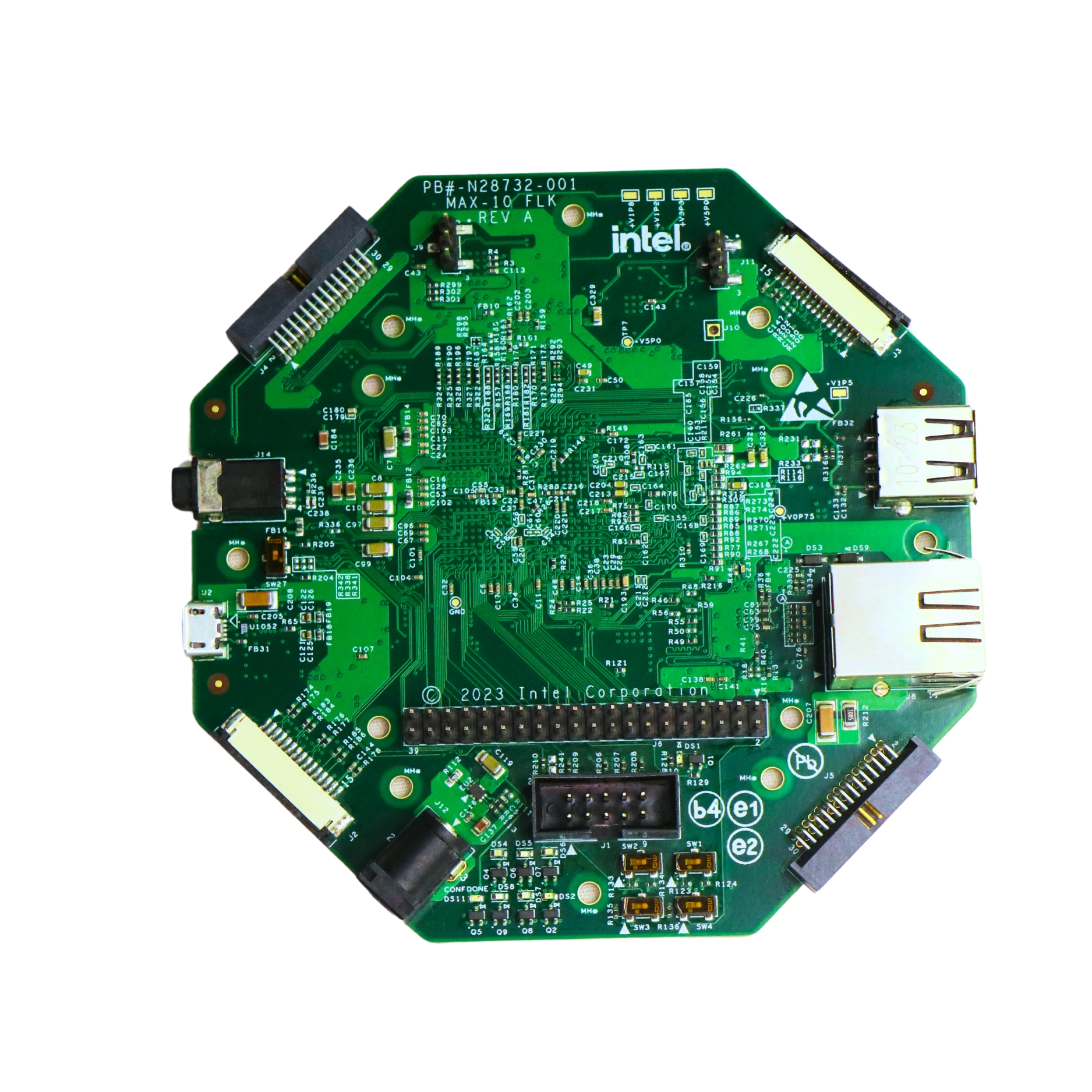
When speed is crucial in digital design, Ripple Carry Adders fall short due to sequential carry delays. The Carry Look-Ahead Adder (CLA) offers a smarter solution by calculating carry bits in parallel. This blog guides you through the CLA concept, Verilog implementation, and simulation steps—ideal for learners working with the MAX10 FLK FPGA board.
What is a Carry Look-Ahead Adder?
A CLA improves speed by using Generate (G) and Propagate (P) logic to calculate all carry signals in parallel. Unlike ripple carry adders, where each bit must wait for the previous carry, CLA handles carry prediction ahead of time—minimising delay and enhancing performance.
Generate (G): A carry is generated at this bit position.
Propagate (P): A carry input is passed to the next bit.
Verilog Code: CLA Using Dataflow Modeling
Design Code
// Pantech e-learning
// Carry Look Ahead Adder – Dataflow Modeling
module cla_4bit(
input [3:0] a, b,
input cin,
output [3:0] sum,
output cout
);
wire [3:0] p, g;
wire c1, c2, c3;
assign p = a ^ b;
assign g = a & b;
assign sum[0] = p[0] ^ cin;
assign c1 = g[0] | (p[0] & cin);
assign sum[1] = p[1] ^ c1;
assign c2 = g[1] | (p[1] & g[0]) | (p[1] & p[0] & cin);
assign sum[2] = p[2] ^ c2;
assign c3 = g[2] | (p[2] & g[1]) | (p[2] & p[1] & g[0]) | (p[2] & p[1] & p[0] & cin);
assign sum[3] = p[3] ^ c3;
assign cout = g[3] | (p[3] & g[2]) | (p[3] & p[2] & g[1]) |
(p[3] & p[2] & p[1] & g[0]) |
(p[3] & p[2] & p[1] & p[0] & cin);
endmodule
Testbench
// Pantech e-learning
// Testbench for CLA
module cla_4bit_tb;
reg [3:0] a, b;
reg cin;
wire [3:0] sum;
wire cout;
cla_4bit uut(
.a(a), .b(b), .cin(cin),
.sum(sum), .cout(cout)
);
initial begin
$dumpfile(“dump.vcd”);
$dumpvars(0, cla_4bit_tb);
a = 4’b0000; b = 4’b0000; cin = 0; #10;
a = 4’b0011; b = 4’b0001; cin = 0; #10;
a = 4’b0101; b = 4’b0101; cin = 0; #10;
a = 4’b1111; b = 4’b0001; cin = 0; #10;
a = 4’b1111; b = 4’b1111; cin = 1; #10;
$finish;
end
endmodule
Simulation Output
Observe the waveform using GTKWave (VCD file) and verify correct sum and carry outputs for each input combination. This confirms the CLA’s parallel carry generation.
Figure: Carry Look Ahead Adder simulation output
FAQs
Q1: Why is a CLA faster than a ripple carry adder?
Because it computes all carry outputs in parallel, removing dependency on previous stages.
Q2: What is the role of ‘Generate’ and ‘Propagate’?
Generate means a carry is created at that bit. Propagate means the input carry is passed forward.
Q3: Where is CLA used?
CLA is used in high-performance ALUs, CPUs, and processors requiring fast arithmetic.
Q4: What is the limitation of CLA?
As bit-width increases, logic becomes more complex and harder to scale.
Q5: How many full adders are in a CLA?
It doesn’t use full adders directly; it uses logic gates based on G and P terms.
Conclusion
The Carry Look-Ahead Adder offers a brilliant trade-off between speed and complexity. It is ideal for high-speed VLSI design and digital systems where speed is paramount. Whether you’re designing arithmetic units for an ALU or experimenting on your MAX10 FLK FPGA, CLA is a must-know concept in digital logic.
Call to Action
Try implementing this 4-bit Carry Look-Ahead Adder on a MAX10 FLK FPGA board and experience real-time high-speed addition without ripple delay.
Want more logic circuit simulations? Explore our full Verilog series covering all combinational and sequential circuits—perfect for beginners and aspiring FPGA developers!
About Author:
A. Manikandan is an RTL Engineer at Pantech India Solutions Pvt. Ltd. With a strong passion for digital design ,FPGAs and ASIC bus protocols. he specializes in FPGA and hardware development, sharing insights to bridge the gap between academia and industry.
You can adjust the second line to reflect any specific expertise or areas of interest you wish to highlight!
Looking Ahead: Collaborate With Us
- Try building this Full Adder on the Intel MAX10 FLK FPGA board and visualize the simulation results in real-time.
- Want to build a complete multi-bit adder? Explore our beginner-friendly Verilog series at Pantech eLearning.
- Looking for hands-on training? Join our FPGA/VLSI Internship Program and take your digital design skills tothe next level!
- Email: sales@pantechmail.com
- Website: pantechelearning.com
- Exploring EV models & Battery Management Systems
- Deep dive into autonomous systems & Steer-by-Wire tech
Let’s innovate together—and prepare the next generation of tech leaders.
Digital Electronics
Digital electronics
click here
Boolean Algebra and Logic Gates.
click here...
Implementing and Simulating the OR Gate.
click here
Designing XOR Logic in Verilog
click here
Building the NOR Gate in Verilog
click here
Designing the NAND Gate.
click here
Designing a Half Adder in Verilog
click here
Building a Ripple Carry Adder in Verilog.
click here
Designing a 2x1 Multiplexer in Verilog
click here
Carry look ahead.
click here
Comparator in verilog.
click here
Decoder
click here
Designing a Binary Adder
click here

- All Projects
- Product