Designing a 2x1 Multiplexer in Verilog: Simplifying Input Selection
Description
Learn how a 2×1 multiplexer (MUX) works and implement it using Verilog behavioral modelling. Includes testbench, truth table, and simulation output.
Introduction
A multiplexer, or MUX, is a fundamental combinational circuit widely used in digital design. It acts as a data selector, choosing one input from multiple options based on a control (select) signal. In this blog, you’ll learn how a 2×1 MUX operates, write Verilog code for it, and simulate the design using a testbench. This is an essential building block for engineers working on digital systems, FPGA projects, or preparing for VLSI labs.
What is a Multiplexer (MUX)?
A multiplexer is a logic circuit that selects one of several input signals and forwards it to a single output line. The selection is done using select lines.
Key Features
- A 2×1 multiplexer has 2 data inputs, 1 select line, and 1 output.
- Depending on the select line value, either i0 or i1 is passed to the output.
- For n select lines, the MUX can control 2ⁿ inputs.
Truth Table of 2×1 Multiplexer
Select (s) | Input i0 | Input i1 | Output y |
0 | 0 | X | 0 |
0 | 1 | X | 1 |
1 | X | 0 | 0 |
1 | X | 1 | 1 |
Verilog Code for 2×1 Multiplexer
// Pantech e-learning
// 2×1 MUX implementation using behavioral modelling
module mux_2x1(
input s,
input i0,
input i1,
output reg y);
always @(*) begin
y = (s == 1) ? i1 : i0;
end
endmodule
Testbench Code for 2×1 MUX
// Pantech e-learning
module tb_mux_2x1;
reg s, i0, i1;
wire y;
mux_2x1 uut(.s(s), .i0(i0), .i1(i1), .y(y));
initial begin
$dumpfile(“dump.vcd”);
$dumpvars(0, tb_mux_2x1);
$monitor(“Time = %0t | s = %b, i0 = %b, i1 = %b ,output y = %b”, $time, s, i0, i1, y);
s = 1’b0; i0 = 1’b0; i1 = 1’b0;
#10 s = 1’b0; i0 = 1’b1; i1 = 1’b0;
#10 s = 1’b1; i0 = 1’b1; i1 = 1’b0;
#10 s = 1’b1; i0 = 1’b1; i1 = 1’b1;
#10;
$finish;
end
endmodule
Simulation Output
After simulation using a tool like GTKWave or ModelSim, you’ll see that the output y correctly reflects the value of i0 when s = 0, and i1 when s = 1.
Figure 1: 2×1 Mux simulation output log file
Figure 2: 2×1 Mux simulation output waveform
Applications of Multiplexer
- Used in digital data routing
- Essential in communication systems
- Widely used in control logic design
- Forms the core of ALU designs in processors
Frequently Asked Questions (FAQs)
Q1: What is a multiplexer (MUX)?
A MUX is a logic device that selects one input from many and directs it to a single output line using select signals.
Q2: How many inputs does a 2×1 MUX have?
A 2×1 multiplexer has 2 inputs, 1 select line, and 1 output.
Q3: What happens when the select line is 0?
The output is equal to input i0.
Q4: And when the select line is 1?
The output becomes equal to input i1.
Q5: Where are multiplexers commonly used?
MUXes are used in data routing, switching, ALUs, and digital communication circuits.
Conclusion
You’ve just learned how to implement a 2×1 multiplexer using Verilog. Multiplexers are simple yet powerful components in digital system design, and understanding them is crucial for FPGA programming and VLSI logic development.
Call to Action
Want to see it in action?
Run the 2×1 MUX Verilog Code on EDA Playground and observe how the output responds to different select line inputs in real-time.
Looking to master digital circuits with ease?
Join our FPGA & Verilog Internship Program at Pantech eLearning and start building real-world projects from day one.
About Author:
A. Manikandan is an RTL Engineer at Pantech India Solutions Pvt. Ltd. With a strong passion for digital design ,FPGAs and ASIC bus protocols. he specializes in FPGA and hardware development, sharing insights to bridge the gap between academia and industry.
You can adjust the second line to reflect any specific expertise or areas of interest you wish to highlight!
Looking Ahead: Collaborate With Us
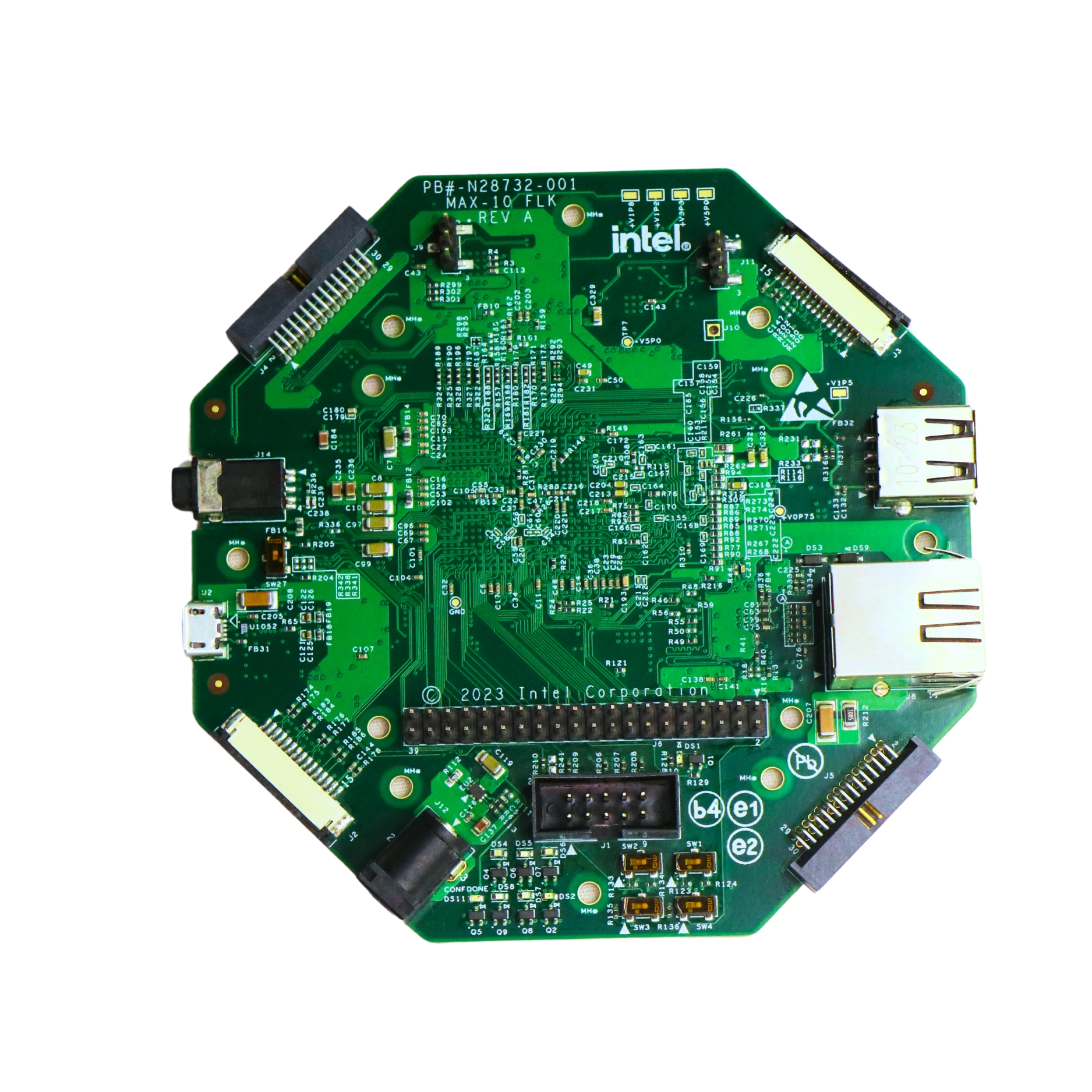
- Try building this Full Adder on the Intel MAX10 FLK FPGA board and visualize the simulation results in real-time.
- Want to build a complete multi-bit adder? Explore our beginner-friendly Verilog series at Pantech eLearning.
- Looking for hands-on training? Join our FPGA/VLSI Internship Program and take your digital design skills tothe next level!
- Email: sales@pantechmail.com
- Website: pantechelearning.com
- Exploring EV models & Battery Management Systems
- Deep dive into autonomous systems & Steer-by-Wire tech
Let’s innovate together—and prepare the next generation of tech leaders.
Digital Electronics
Digital electronics
click here
Boolean Algebra and Logic Gates.
click here...
Implementing and Simulating the OR Gate.
click here
Designing XOR Logic in Verilog
click here
Building the NOR Gate in Verilog
click here
Designing the NAND Gate.
click here
Designing a Half Adder in Verilog
click here
Building a Ripple Carry Adder in Verilog.
click here
Designing a 2x1 Multiplexer in Verilog
click here
Carry look ahead.
click here
Comparator in verilog.
click here
Decoder
click here
Designing a Binary Adder
click here

- All Projects
- Product