The OR gate is a fundamental logic gate used extensively in digital systems. It outputs a logic high (1) when at least one of its inputs is high. This simple yet powerful gate is crucial in control logic, decision-making circuits, alarms, and arithmetic designs. In this blog, we will cover the OR gate’s Verilog implementation, simulate it using a testbench, and explain its practical applications in digital electronics.
Truth Table
A | B | Output (A OR B) |
0 | 0 | 0 |
0 | 1 | 1 |
1 | 0 | 1 |
1 | 1 | 1 |
Verilog Design Code
// Pantech e-learning
// OR gate using dataflow modeling
module or_gate(
input a,
input b,
output y
);
assign y = a | b;
endmodule
Testbench Code
// Pantech e-learning
module or_gate_tb;
reg a, b;
wire y;
or_gate uut (
.a(a),
.b(b),
.y(y)
);
initial begin
$dumpfile(“dump.vcd”);
$dumpvars(0, or_gate_tb);
a = 0; b = 0; #10;
a = 0; b = 1; #10;
a = 1; b = 0; #10;
a = 1; b = 1; #10;
$finish;
end
endmodule
Waveform Output
In the simulation waveform, the output y is 1 whenever at least one input (a or b) is 1, validating the OR gate’s logic operation.

Figure: OR gate simulation waveform
Applications
• Used in decision-making logic such as security alarms
• Implemented in digital control circuits for selecting multiple enable signals
• Integral in arithmetic units and adders
• Employed in condition-checking logic within processors
• Used in programmable logic arrays and combinational logic circuits
Frequently Asked Questions (FAQs)
Q1: Can we use or as a module name in Verilog?
A1: No, or is a reserved keyword. Use names like or_gate or my_or instead.
Q2: What happens if one input is unknown (X) in an OR gate?
A2: If one input is X and the other is 0, the output is X. But if one input is 1, the output is 1 since 1 OR X results in 1.
Q3: What is the difference between wire and reg in Verilog?
A3: wire is for continuous assignments (like assign statements), while reg is used in procedural blocks such as initial and always.
Q4: How can an OR gate be implemented using gate-level modeling in Verilog?
A4: You can use built-in primitives like:
or (y, a, b);
Q5: Why is it important to test all input combinations in the OR gate testbench?
A5: Testing all input cases (00, 01, 10, 11) ensures the logic behaves correctly under every possible input, guaranteeing accurate functionality.
Conclusion
The OR gate, while simple, is pivotal in designing and controlling digital systems. Simulating and understanding its behavior in Verilog is essential for anyone entering FPGA, ASIC, or digital logic design.
Call to Action
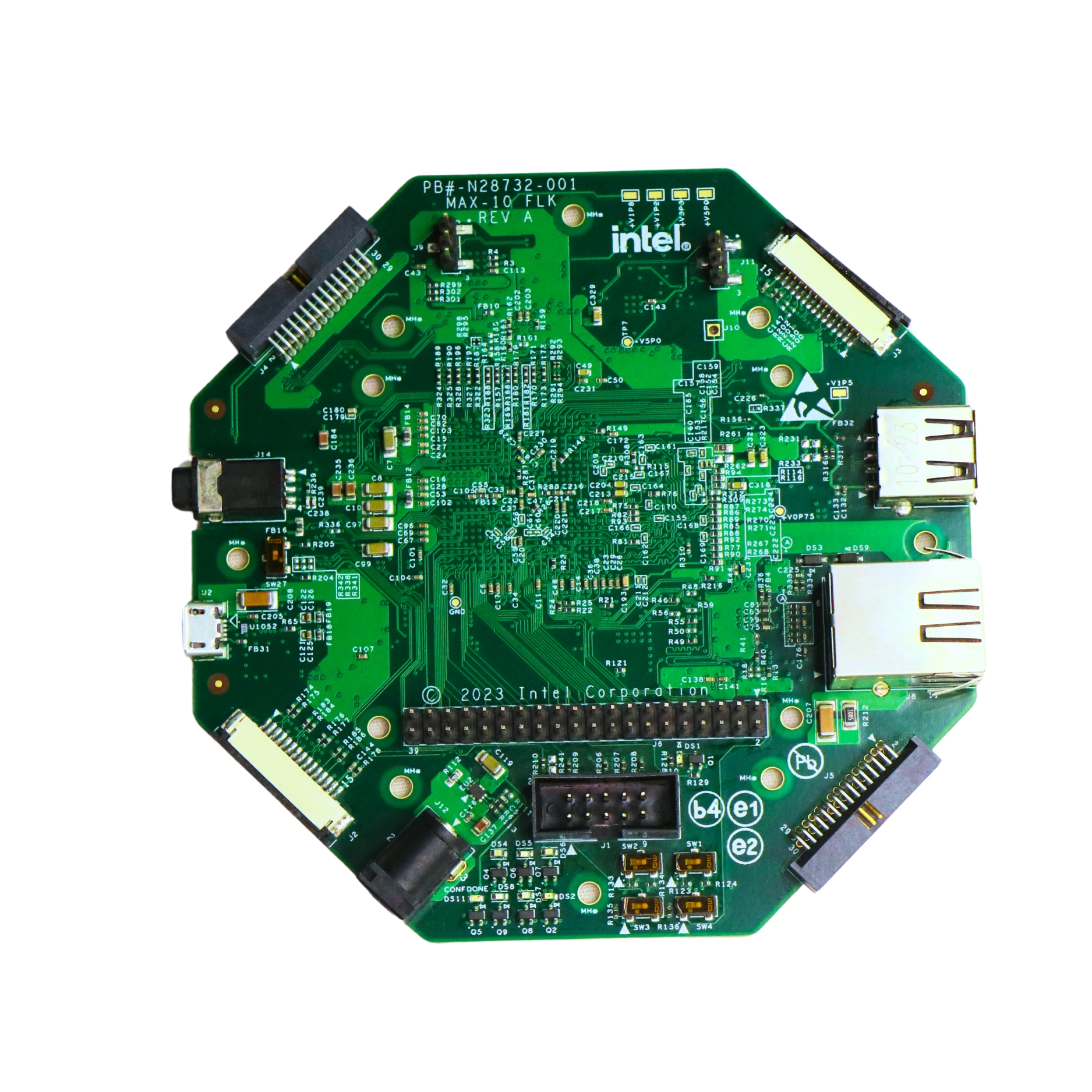
Try running this OR gate project on an Intel MAX10 FPGA board or simulate it on EDA Playground.
Want to go deeper? Explore our next blog on implementing NAND gates and building a complete logic gate library in Verilog!
- All Projects
- Product