Truth Table
A | B | A NAND B |
0 | 0 | 1 |
0 | 1 | 1 |
1 | 0 | 1 |
1 | 1 | 0 |
Verilog Design Code
// Pantech e-learning
// NAND gate using dataflow modeling
module nand_gate(
input a,
input b,
output y
);
assign y = !(a & b);
endmodule
Testbench Code
// Pantech e-learning
module nand_gate_tb;
reg a, b;
wire y;
nand_gate uut(
.a(a),
.b(b),
.y(y)
);
initial begin
$dumpfile(“dump.vcd”);
$dumpvars;
a = 1’b0; b = 1’b0;
#10 a = 1’b0; b = 1’b1;
#10 a = 1’b1; b = 1’b0;
#10 a = 1’b1; b = 1’b1;
#10 $finish;
end
endmodule
Waveform Output
The output waveform clearly shows high (1) output for all cases except when both inputs are 1, which results in a low (0)—validating the NAND gate behavior.

Figure: NAND gate simulation output
Applications
- Used in memory circuits like SRAM and DRAM
- Core of universal gate logic design
- Found in timers and oscillators
- Preferred in CMOS design due to lower transistor count
- Helps build combinational and sequential circuits
Frequently Asked Questions (FAQs)
Q1: Why is the NAND gate considered efficient in digital design?
A1: It uses fewer transistors and is capable of implementing any logic function, saving space and cost.
Q2: What happens if both NAND gate inputs are unknown (X)?
A2: The output becomes X, signaling uncertainty and aiding in simulation debugging.
Q3: Can a NAND gate be used to create other gates?
A3: Yes, it’s a universal gate that can construct NOT, AND, OR, XOR, and more.
Q4: What is the output if one input is 0 and the other is X?
A4: Output is 1 since 0 AND X equals 0, and NAND inverts that to 1.
Q5: Why use a NAND gate instead of an AND gate in fault-tolerant logic?
A5: NAND’s default output is 1, which is often considered a safe or inactive state, making it safer in critical systems.
Conclusion
The NAND gate is not just a basic digital component—it is a gateway to building complex logic using simple principles. By simulating it in Verilog and observing its behavior, you’ve taken a key step toward mastering digital design.
Call to Action
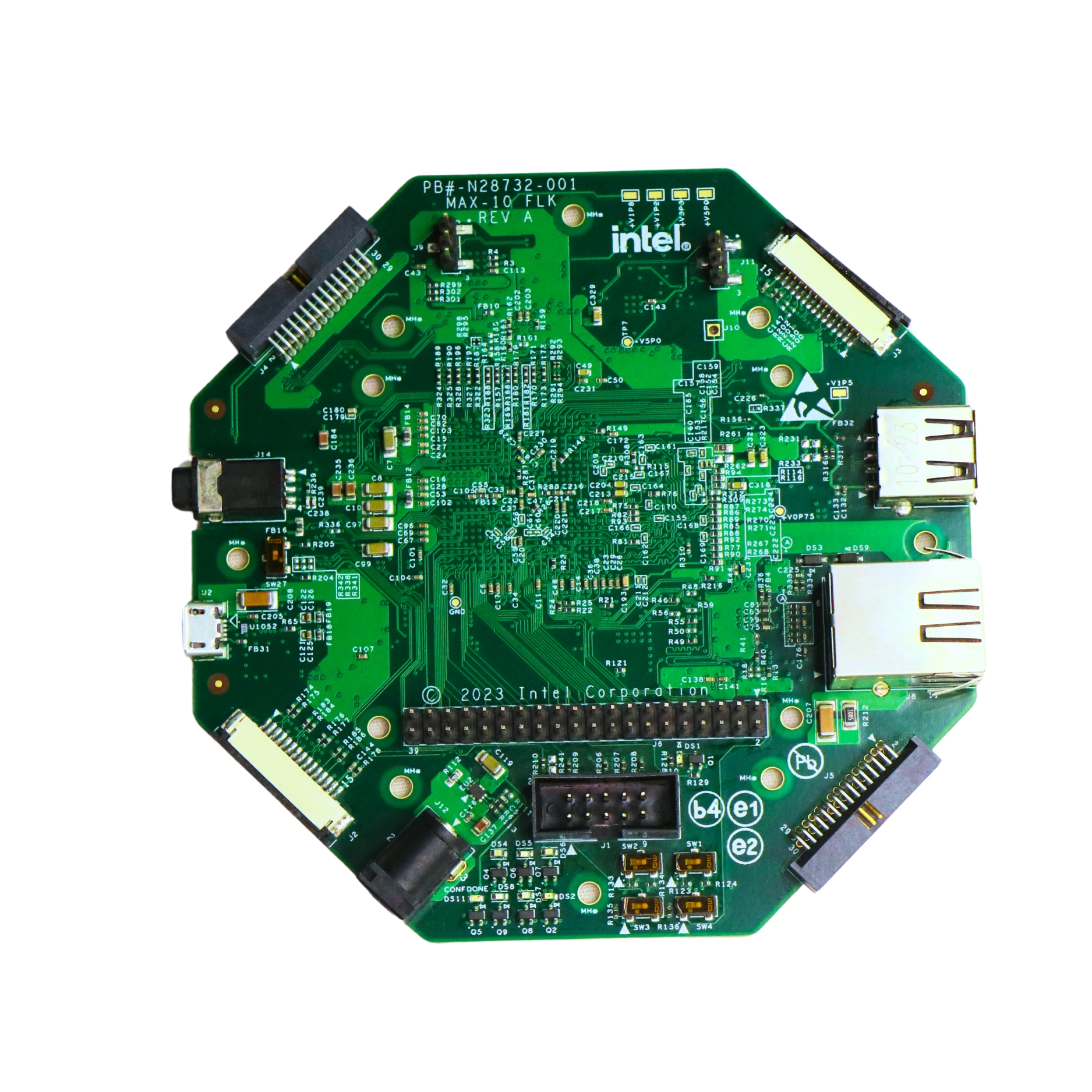
Experiment further by deploying this design on a MAX10 FLK FPGA board from Pantech eLearning.
Looking to deepen your Verilog skills? Join our hands-on FPGA internship program today.
- All Projects
- Product