Core Sections
Concept Explanation
A NOR gate performs a logical NOT of the OR operation. That means the output is 1 only when all inputs are 0. In every other case, the output will be 0.
Truth Table:
|
A |
B |
A NOR B |
|
0 |
0 |
1 |
|
0 |
1 |
0 |
|
1 |
0 |
0 |
|
1 |
1 |
0 |
Implementation
Verilog Design Code
// Pantech e-learning
// NOR gate using dataflow modeling
module nor_gate(
input a,
input b,
output y
);
assign y = !(a | b);
endmodule
Testbench Code
// Pantech e-learning
module nor_gate_tb;
reg a, b;
wire y;
nor_gate uut (
.a(a),
.b(b),
.y(y)
);
initial begin
$dumpfile(“dump.vcd”);
$dumpvars;
a = 0; b = 0;
#10 a = 0; b = 1;
#10 a = 1; b = 0;
#10 a = 1; b = 1;
#10 $finish;
end
endmodule
Waveform Output
The simulation confirms that the NOR gate behaves as expected: the output remains high (1) only when both inputs are low. The Verilog code was simulated using EDAPlayground, and waveforms were visualized through EPWave, helping students confirm the logic visually.

Figure: NOR gate
Applications
- Used in digital comparators and memory circuits
- Fundamental in latch and flip-flop designs
- Used for creating any other logic gate (AND, OR, NOT, XOR)
- Integrated in alarm circuits and safety systems
Frequently Asked Questions (FAQs)
Q1: What does the output of a NOR gate indicate in terms of input conditions?
A1: The output is 1 only when both inputs are 0; otherwise, it’s 0.
Q2: In Verilog simulation, how does a NOR gate behave with uninitialized inputs?
A2: The output may show X (unknown), helping detect uninitialized or faulty signals.
Q3: Can a NOR gate be used to construct other gates?
A3: Yes, it is a universal gate and can replicate the behavior of any basic logic gate.
Q4: What happens if one input is 1 and the other is unknown (X)?
A4: The OR operation evaluates to 1, so the NOR output becomes 0 regardless of the unknown.
Q5: How is the NOR gate represented using behavioral modeling in Verilog?
A5: It can be written as y = ~(a | b); inside an always @(*) block.
Conclusion
You’ve now learned how to design, simulate, and verify the working of a 2-input NOR gate using Verilog. This logic gate is not only important on its own but also serves as a building block for more complex systems. Mastering it lays the groundwork for your digital design journey.
Call to Action (CTA)
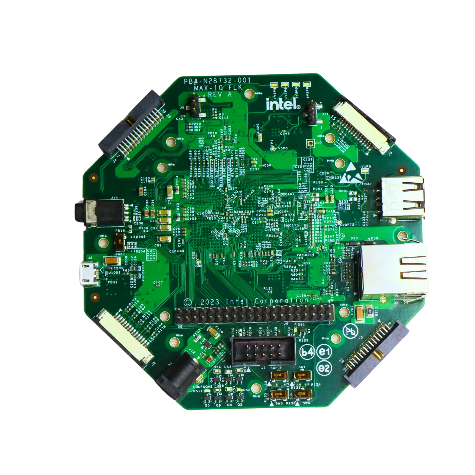
- Test this NOR gate project on the MAX10 FLK FPGA Development Kit, available through Pantech eLearning.
- Join our FPGA & VLSI Internship Program to explore more hands-on logic design using Verilog and Intel MAX10 boards.
- All Projects
- Product