Vlsi design
Internship 2025
Equips you with the skills to design, code, and implement FPGA-based digital systems. Gain hands-on experience and the knowledge to confidently tackle complex projects in VLSI and FPGA domains, applying these concepts to create efficient, real-time, and practical solutions.
1/ 2 Months
Online
8+ Live Projects
Dual Certification
Ultimate Step towards your Career Goals: Expert in VLSI Design
Internship Benifits
Mentorship
Receive guidance and insights from industry experts.
Hands-on Experience
Gain practical skills in a real-world cutting-edge projects.
Networking
Connect with professionals and peers in your field.
Skill Development
Enhance your technical and soft skills.
Career Advancement
Boost your resume with valuable experience.
Certificate
Get a certification to showcase your achievements.
VLSI Internship Overview
The core principles of Very-Large-Scale Integration (VLSI) and Field Programmable Gate Arrays (FPGA), focusing on how they are revolutionizing industries from electronics to telecommunications. Understanding the essential differences and similarities between VLSI and FPGA and exploring how FPGAs provide the flexibility of reprogrammable logic while delivering high performance.
- Intel Quartus Tool Setup: Step-by-step guidance on setting up the Intel Quartus tool, essential for developing and simulating FPGA designs.
- MAX10 FPGA FLK Board: Overview of the MAX10 FPGA FLK Board, highlighting its features and capabilities in supporting entry-level to advanced projects.
- Digital Electronics Fundamentals: This foundational section covers logic gates, switching circuits, and other basic digital elements. You’ll learn how to design and interpret basic combinational circuits, which form the basis of more complex digital systems.
The fundamental building blocks of digital systems: flip-flops, registers, counters, and digital memory. Through hands-on examples, you’ll understand how these elements store and process data in digital circuits.
- Flip-Flops and Registers: Dive into the inner workings of various types of flip-flops (e.g., D, T, JK) and registers, exploring how they are used for data storage and manipulation in digital systems.
- Counters and Digital Memory: Understand the design of counters and their role in sequential logic. Learn how digital memory functions and how counters are used in practical applications.
- Introduction to Verilog: Get acquainted with the Verilog hardware description language, which is widely used for digital circuit design. You’ll learn the syntax, data types, and basic structures in Verilog, which will serve as the foundation for coding digital systems.
Three primary Verilog modeling styles: gate-level, dataflow, and behavioral. Each style offers a different level of abstraction, allowing you to design circuits in the way that best suits the application.
- Gate-Level Modeling: Learn how to represent circuits at the transistor level, ideal for highly detailed and optimized designs.
- Dataflow and Behavioral Modeling: Understand dataflow modeling for defining the flow of data between modules, and behavioral modeling for defining the behavior of systems without focusing on low-level details.
- Practical Verilog Coding: Through hands-on projects, apply these modeling styles to design combinational and sequential circuits, including latches, flip-flops, and shift registers. This module bridges the gap between theory and practical application by enabling you to simulate and test designs in Quartus.
Explores Finite State Machines (FSMs), a powerful concept used to model sequential logic circuits.
Two types of FSMs — Moore and Mealy machines — and their applications in digital design.
- Moore FSMs: Study FSMs where the outputs depend solely on the current state, making them ideal for synchronous designs where stability is crucial.
- Mealy FSMs: Understand FSMs where outputs depend on both the current state and current inputs, allowing for more responsive designs.
- Verilog Coding for FSMs: Through coding exercises, you’ll design both Moore and Mealy FSMs in Verilog, implementing these designs on the MAX10 FPGA board. The FSM designs will cover practical applications and illustrate how FSMs manage complex state transitions effectively.
Project Implementation and Off-Chip Communicatios and hands-on project that allows you to implement, test, and deploy your designs on the MAX10 FPGA.
- JTAG Programming: Learn how to load your Verilog designs onto the FPGA using the JTAG programming method, enabling you to test your designs on physical hardware.
- GPIO Control: This section introduces General Purpose Input/Output (GPIO) control, allowing you to interact with external devices and sensors via the FPGA.
- UART Communication Protocol: A key focus will be on UART (Universal Asynchronous Receiver-Transmitter) communication, specifically the RX (receive) functionality. Apply UART to interact with off-chip devices, bringing the FPGA design into real-world applications where communication and data transfer are essential.
Looking for in-depth Syllabus Information? Explore your endless possibilities in VLSI with our Brochure!
share this detailed brochure with your friends! Spread the word and help them discover the amazing opportunities awaiting them.
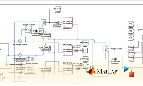
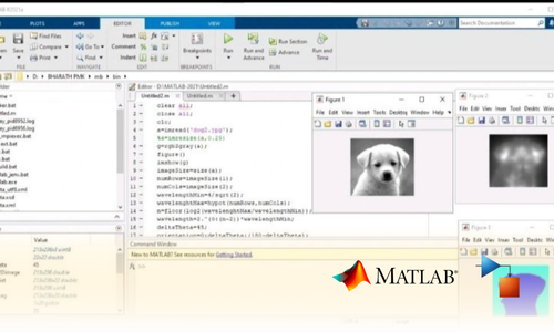
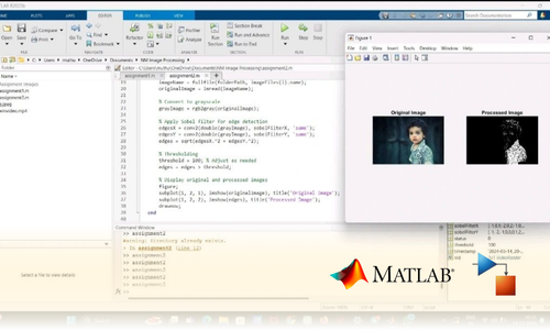
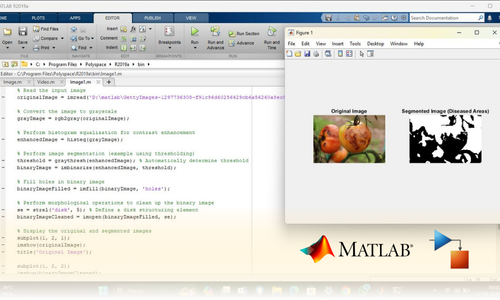
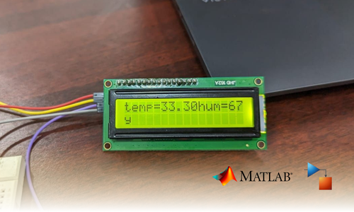
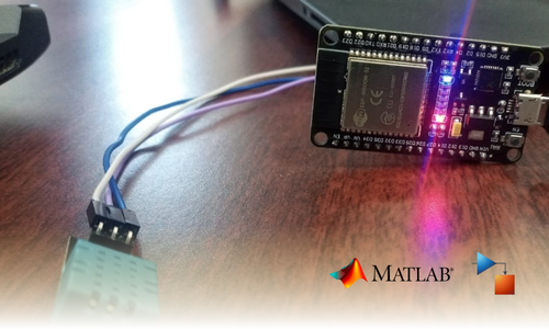
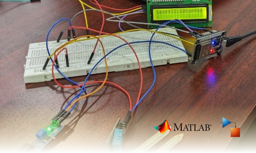
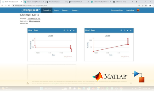
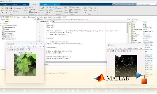
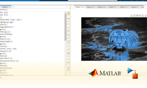
Project Submission: Example Output Screenshots from Our Clients
Take a look at these sample outputs crafted by our clients. These screenshots showcase the impressive results achieved through our courses and projects. Be inspired by their work and visualize what you can create!
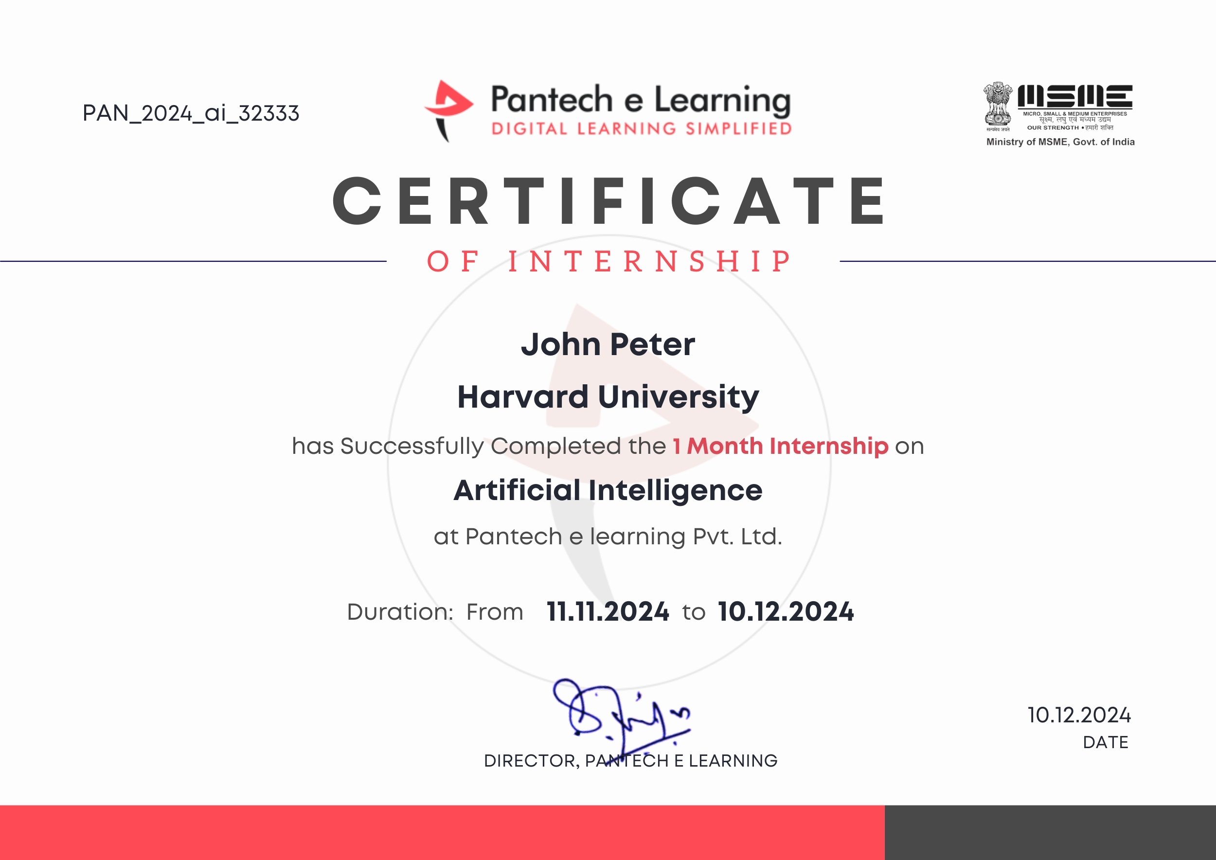
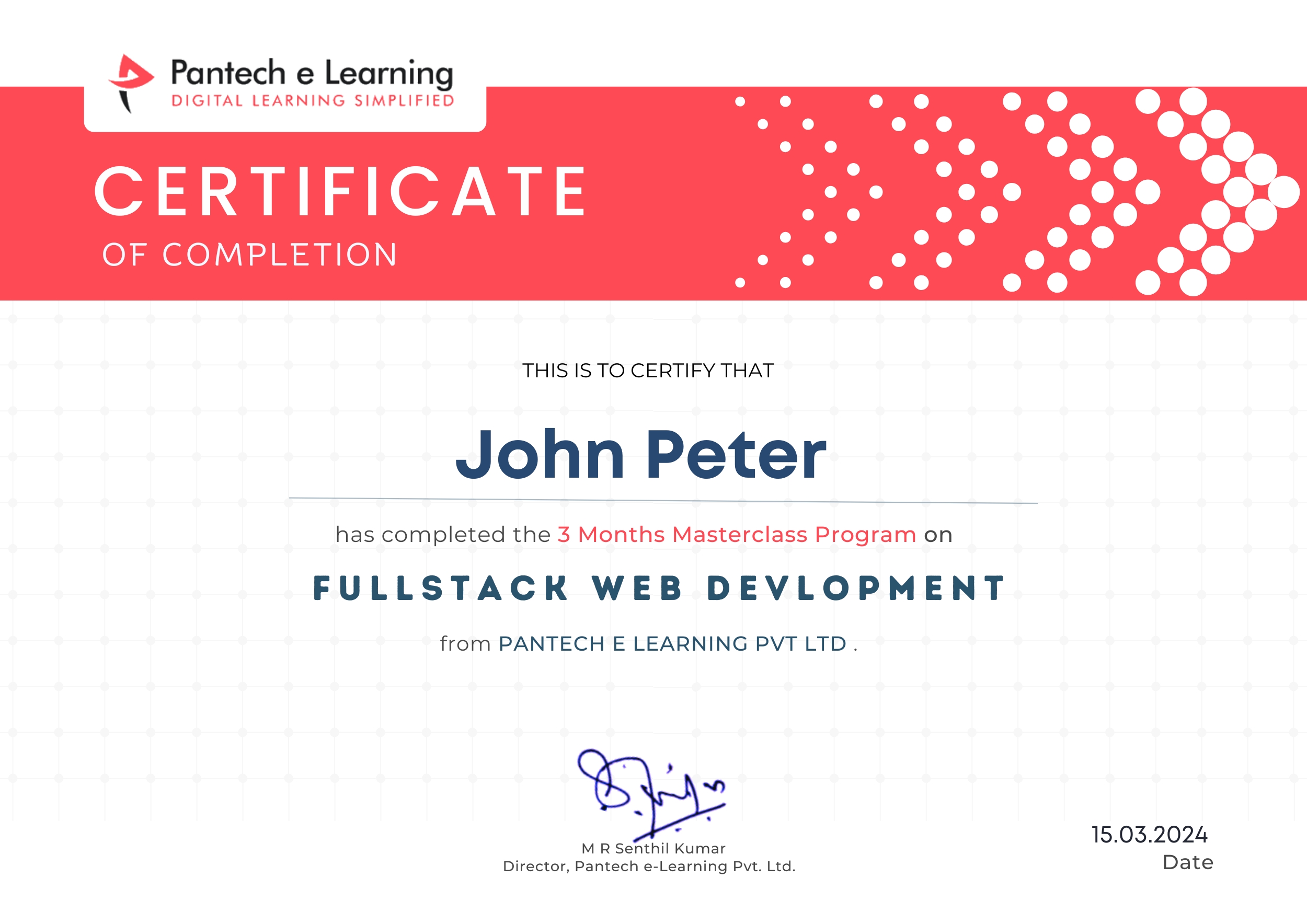
Dual Certification: Internship Completion & Participation
Earn prestigious Dual Certification upon successful completion of our internship program. This recognition validates both your participation and the skills you have honed during the internship
How does this Internship Program Work?
Step 1 Enroll in the Program
- Get a Mentor Assigned
- Presentations & Practice Codes
- Learn at your Flexible Time
- Apprehend the concepts
Step 2 Project Development
- Implement Skills Learn
- Develop Projects with assistance
- Get Codes for Reference
- Visualise the Concepts
Step 3 Get Certified
- Certificate of Internship
- Project Completion Certificate
- Share on social media
- Get Job Notifications
Choose Your Plan fit your needs
Master the Latest Industrial Skills. Select a technology domain & kick off your Internship immediately.
1 Month
₹1999/-
₹999/-
- Internship Acceptance Letter
- 90 Days from the date of payment
- 4 LIVE intractive Mastermind Sessions
- 4+ Capstone Projects & Codes
- Full Roadmap
- Internship Report
- 1 Month Internship Certificate
2 Month
₹3299/-
₹1899/-
- Internship Acceptance Letter
- 180 Days from the date of payment
- 4 LIVE interactive Mastermind Sessions
- 12+ Capstone Projects & Codes
- Full Roadmap
- Internship Report
- Participation Certificate
- 2 Month Internship Certificate
Our Alumni Employers
Curious where our graduates make their mark? Our students go on to excel in leading tech companies, innovative startups, and prestigious research institutions. Their advanced skills and hands-on experience make them highly sought-after professionals in the industry.




EXCELLENTTrustindex verifies that the original source of the review is Google. I recently completed my Python internship under the guidance of Mentor poongodi mam We learnt so many new things that developed my knowledge.this experience is good to learnTrustindex verifies that the original source of the review is Google. I completed my python internship guidance of mentor poongodi mam. She thought us in friendly qayTrustindex verifies that the original source of the review is Google. Poongodi mam done very well She took the class very well When we ask any doubt without getting bored she will explain,we learned so much from mam,marvelousTrustindex verifies that the original source of the review is Google. I have handled by poongodi mam.domain python intership...was goodTrustindex verifies that the original source of the review is Google. I recently completed Python internship under the guidance of poongodi mam who excelled in explaining concepts in an easily understandable wayTrustindex verifies that the original source of the review is Google. Fantastic class we were attended..we got nice experience from this class..thank you for teaching python mam...Trustindex verifies that the original source of the review is Google. -The course content was well-structured - I gained valuable insights into microcontrollers, sensors, and programming languages- The workshop was informative, interactive, and challenging, pushing me to think creatively. Ms Jimna our instructor her guidance and feedback helped me overcome obstacles and improve my skills.Trustindex verifies that the original source of the review is Google. The learning experience was really worth since more than gaining just the knowledge all of the inputs were given in a friendly and sportive manner which then made it a good place to learn something with a free mindset... 👍🏻Trustindex verifies that the original source of the review is Google. I recently completed my full stack python intership under the guidance of mentor Gowtham,who excelled in explaining concepts in an easily understand mannerTrustindex verifies that the original source of the review is Google. Gowtham-very interesting class and I learning so many things in full stack python development and I complete my internship in Pantech e learning and it is useful for my career
FAQ
What topics are covered in the VLSI & FPGA program?
This Internship covers digital circuit design, Verilog programming, FSMs, GPIO control, and communication protocols like UART. Work with MAX10 FPGA hardware and Intel Quartus software to implement real-world projects.
Do I need prior experience with VLSI or FPGA?
No prior experience is required. The program is designed for beginners, starting with basic concepts and progressing to more advanced topics in VLSI and FPGA design.
What hardware and software tools will be used?
Use the Intel Quartus tool for FPGA programming and the MAX10 FPGA FLK Board for hands-on experiments, along with other tools for circuit design and testing.
What is a Finite State Machine (FSM) and how is it used?
An FSM is a computational model used to design sequential circuits, where the output depends on the current state. It’s commonly used for control systems, communication protocols, and more.
What are the benefits of using an FPGA over other microcontrollers?
FPGAs offer higher flexibility, parallel processing, and faster data handling than microcontrollers, making them ideal for complex and high-performance applications.
Do I need to buy any software for this course?
You can download Intel Quartus for free. Additional software tools and resources will be provided during the course.
Start Your Tech Journey Today
Sign Up for Exclusive Resources and Courses Tailored to Your Goals!
© 2025 pantechelearning.com

