

PCB DESIGN
Internship 2025
Career-Based Complete PCB Design Internship Program. Get Insights into: Schematic, Footprint, Single Layer, Double Layer, Cadance concepts with Project Implementation and Assignments. Stay Updated on Latest Industrial Updates.
1/ 2 Months
Online
8+ Live Projects
Dual Certification
Ultimate Step towards your Career Goals: Expert in PCB Design
Get ahead with the FutureTech Industrial Internship Program: gain hands-on experience, connect with industry leaders, and develop cutting-edge skills. Earn a stipend, receive expert mentorship, and obtain a certificate to boost your career prospects. Transform your future with practical, real-world learning today
Internship Benifits
Mentorship
Receive guidance and insights from industry experts.
Hands-on Experience
Gain practical skills in a real-world cutting-edge projects.
Networking
Connect with professionals and peers in your field.
Skill Development
Enhance your technical and soft skills.
Career Advancement
Boost your resume with valuable experience.
Certificate
Get a certification to showcase your achievements.
PCB Design Internship Overview
The concept of Printed Circuit Boards (PCBs) and their applications. PCBs are fundamental components in electronics, providing both mechanical support and electrical connections for various electronic components. The section covers the essential aspects of PCBs, including:
- Overview of PCB Design: A brief explanation of the PCB design process, which involves creating a schematic diagram, selecting components, creating footprints, routing connections, and generating the final files required for manufacturing the board.
- Applications: PCBs are used in a wide range of applications, from simple consumer electronics to complex industrial systems, medical devices, automotive electronics, and communication devices.
The creation of the schematic diagram, which is a visual representation of the electrical connections between various components in the PCB design process. The schematic serves as the blueprint for the board and helps designers:
- Create Schematic Diagram: Using tools like Cadence OrCAD or KiCad, designers draw the circuit with symbols representing components such as resistors, capacitors, and integrated circuits.
- Define Electrical Connections: The schematic diagram defines how the components are connected electrically, ensuring that signals and power are routed correctly.
- Simulation and Validation: Before proceeding with the physical design, the schematic is often simulated to verify functionality and identify errors in logic or connections.
The focus is on translating the schematic components into their physical counterparts on the PCB. This involves creating footprints and generating important data files like BOM (Bill of Materials) and Netlist:
- Footprint Creation: A footprint is a physical layout of the component on the PCB, which defines the size, shape, and pinout of components like resistors, capacitors, connectors, and ICs. Each footprint corresponds to a specific component in the schematic.
- BOM Creation: The Bill of Materials lists all the components used in the design, including part numbers, values, and quantities, which helps during the PCB assembly process.
- Netlist Creation: The Netlist is a data file that lists all the electrical connections between components. It is used to ensure that the routing of the PCB matches the schematic.
The design and routing of a Single Layer PCB, which is a board with electrical connections made on a single side. Key tasks in this section include:
- Single Layer PCB Creation: The designer places components on the PCB, ensuring they are appropriately spaced and aligned according to design rules.
- Component Placement: Placement of components is crucial for optimal routing, signal integrity, and minimizing interference. Placement also affects factors like manufacturability and cost.
- Routing: The process of connecting the components using copper traces is referred to as routing. In a single-layer PCB, traces must be routed on the same surface as the components. The routing process involves considering factors like trace width, spacing, and impedance.
- Gerber Creation: After routing, the final step involves generating Gerber files, which are the standard format used for PCB fabrication. Gerber files define the copper layers, drill holes, silkscreen, and other aspects of the board layout.
Double Layer PCB Design: A double-layer PCB uses both sides of the board for routing electrical connections. This allows for more complex designs compared to single-layer PCBs, as designers can use both sides for component placement and routing.
Schematics, BOM & Footprint: Similar to single-layer designs, double-layer PCBs require careful schematic, footprint, and BOM management.
Component Placement & Routing: The design process is more complex due to the need to manage routing on two layers. Tools such as Cadence Allegro or Altium Designer help automate some aspects of this process.
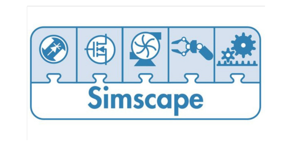
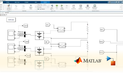
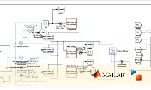
MATLAB & Simscape: MATLAB and Simscape are used to simulate and model various systems, including battery packs. This section covers:
Constructing Battery Pack Simulations: Simscape allows for the simulation of electrical systems like battery packs to assess their performance under different conditions, such as charging/discharging cycles, thermal management, and efficiency.
Simulation for Design Validation: Simulating battery packs and other systems in Simscape helps ensure that the design meets the required performance criteria before physical testing or production. It can simulate battery charge/discharge curves, efficiency, and life-cycle prediction.


Looking for in-depth Syllabus Information? Explore your endless possibilities in PCB Design with our Brochure!
share this detailed brochure with your friends! Spread the word and help them discover the amazing opportunities awaiting them.
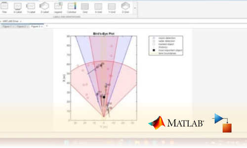
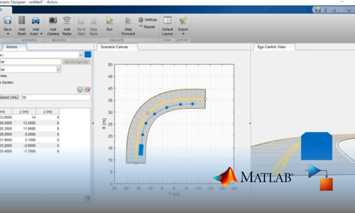
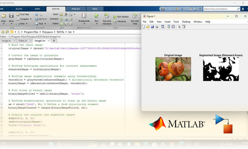
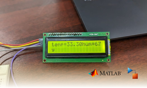
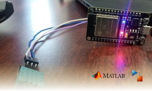
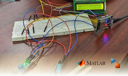
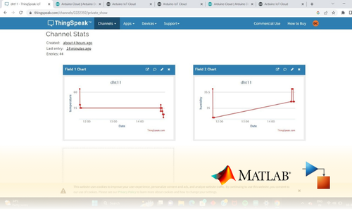
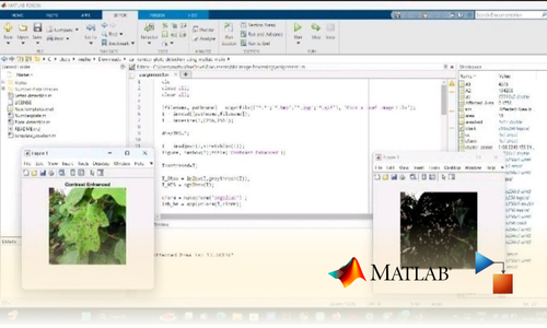
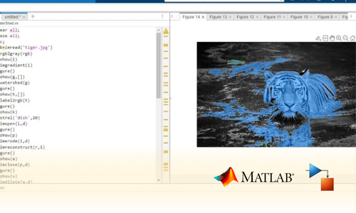
Project Submission: Example Output Screenshots from Our Clients
Take a look at these sample outputs crafted by our clients. These screenshots showcase the impressive results achieved through our courses and projects. Be inspired by their work and visualize what you can create!
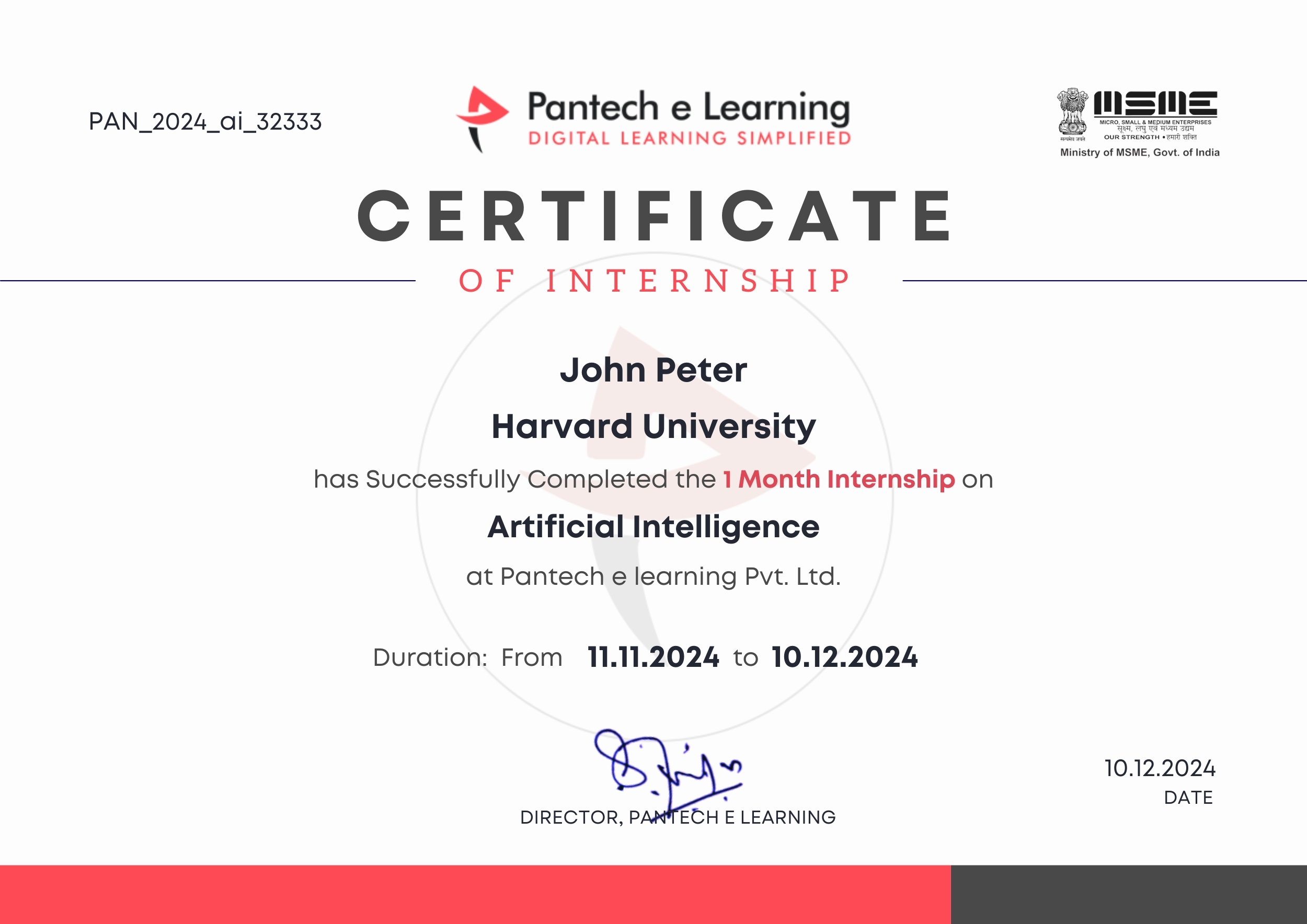
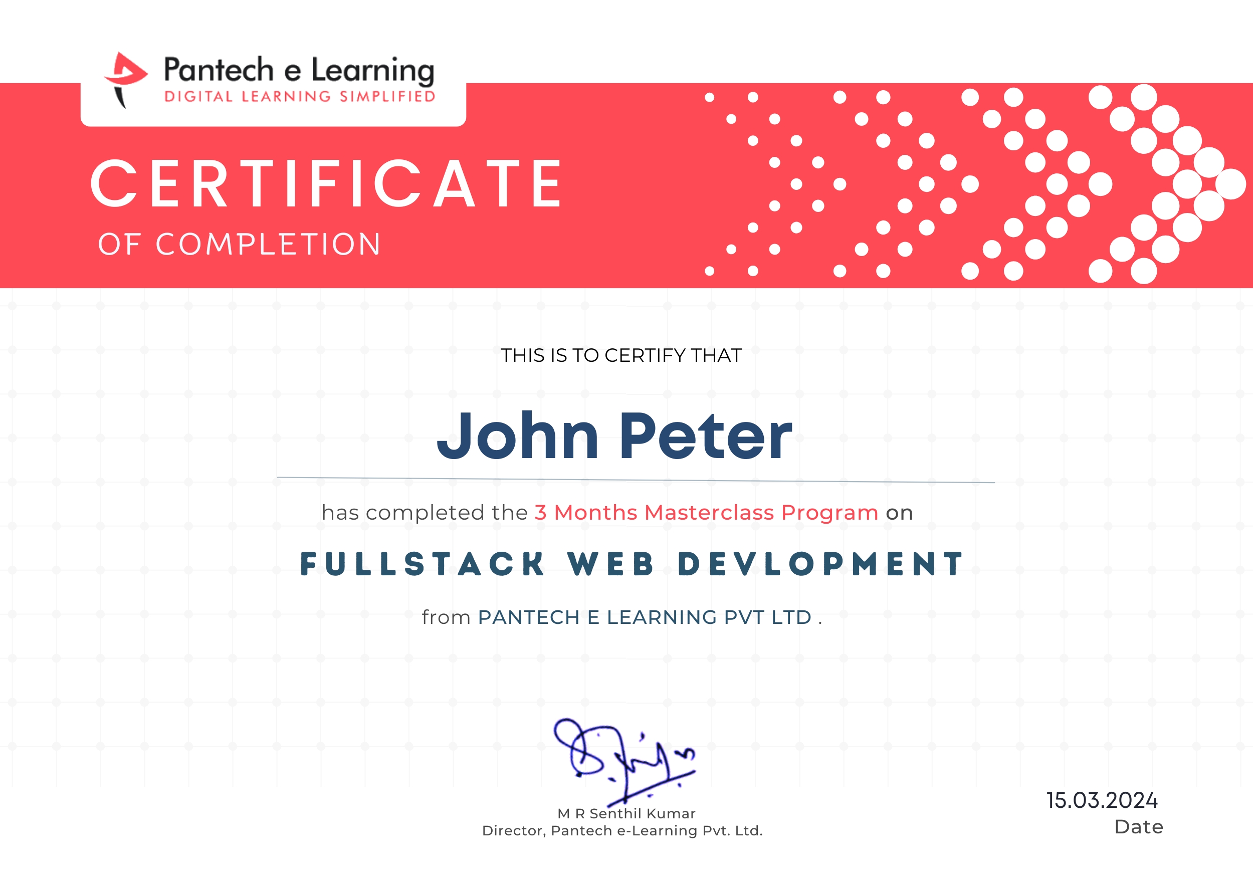
Dual Certification: Internship Completion & Participation
Earn prestigious Dual Certification upon successful completion of our internship program. This recognition validates both your participation and the skills you have honed during the internship
How does this Internship Program Work?
Step 1 Enroll in the Program
- Get a Mentor Assigned
- Presentations & Practice Codes
- Learn at your Flexible Time
- Apprehend the concepts
Step 2 Project Development
- Implement Skills Learn
- Develop Projects with assistance
- Get Codes for Reference
- Visualise the Concepts
Step 3 Get Certified
- Certificate of Internship
- Project Completion Certificate
- Share on social media
- Get Job Notifications
Choose Your Plan fit your needs
Master the Latest Industrial Skills. Select a technology domain & kick off your Internship immediately.
1 Month
₹1999/-
₹999/-
- Internship Acceptance Letter
- 90 Days from the date of payment
- 4 LIVE intractive Mastermind Sessions
- 4+ Capstone Projects & Codes
- Full Roadmap
- Internship Report
- 1 Month Internship Certificate
2 Month
₹3299/-
₹1899/-
- Internship Acceptance Letter
- 180 Days from the date of payment
- 4 LIVE interactive Mastermind Sessions
- 12+ Capstone Projects & Codes
- Full Roadmap
- Internship Report
- Participation Certificate
- 2 Month Internship Certificate
Our Alumni Employers
Curious where our graduates make their mark? Our students go on to excel in leading tech companies, innovative startups, and prestigious research institutions. Their advanced skills and hands-on experience make them highly sought-after professionals in the industry.


EXCELLENTTrustindex verifies that the original source of the review is Google. I recently completed my Python internship under the guidance of Mentor poongodi mam We learnt so many new things that developed my knowledge.this experience is good to learnTrustindex verifies that the original source of the review is Google. I completed my python internship guidance of mentor poongodi mam. She thought us in friendly qayTrustindex verifies that the original source of the review is Google. Poongodi mam done very well She took the class very well When we ask any doubt without getting bored she will explain,we learned so much from mam,marvelousTrustindex verifies that the original source of the review is Google. I have handled by poongodi mam.domain python intership...was goodTrustindex verifies that the original source of the review is Google. I recently completed Python internship under the guidance of poongodi mam who excelled in explaining concepts in an easily understandable wayTrustindex verifies that the original source of the review is Google. Fantastic class we were attended..we got nice experience from this class..thank you for teaching python mam...Trustindex verifies that the original source of the review is Google. -The course content was well-structured - I gained valuable insights into microcontrollers, sensors, and programming languages- The workshop was informative, interactive, and challenging, pushing me to think creatively. Ms Jimna our instructor her guidance and feedback helped me overcome obstacles and improve my skills.Trustindex verifies that the original source of the review is Google. The learning experience was really worth since more than gaining just the knowledge all of the inputs were given in a friendly and sportive manner which then made it a good place to learn something with a free mindset... 👍🏻Trustindex verifies that the original source of the review is Google. I recently completed my full stack python intership under the guidance of mentor Gowtham,who excelled in explaining concepts in an easily understand mannerTrustindex verifies that the original source of the review is Google. Gowtham-very interesting class and I learning so many things in full stack python development and I complete my internship in Pantech e learning and it is useful for my career
FAQ
What is the role of simulation in PCB design?
- Answer: Simulation is used to verify the functionality and performance of the PCB design before manufacturing. This includes:
- Electrical Simulation: Ensuring that the design works as intended, identifying possible issues like short circuits or incorrect connections.
- Thermal Simulation: Assessing how heat will affect components, ensuring that the design can dissipate heat effectively.
- Signal Integrity Simulation: Ensuring that high-speed signals will travel without interference or data loss.
What tools can I use for PCB design and simulation?
Answer: Popular tools for PCB design and simulation include:
- Cadence OrCAD/Allegro: Industry-leading tools for schematic capture, PCB design, and layout.
- Altium Designer: A comprehensive PCB design tool with advanced features for schematic capture and layout.
- KiCad: A free, open-source PCB design tool suitable for hobbyists and professionals.
- MATLAB/Simscape: Used for simulating systems like battery packs and power circuits, useful for evaluating performance before actual design and manufacturing.
Why is component placement so important in PCB design?
Answer: Component placement is critical for:
- Signal Integrity: Placing components close to each other can minimize signal paths, reducing noise and interference.
- Manufacturability: Proper placement ensures that the PCB can be efficiently assembled and soldered.
- Thermal Management: Placing heat-sensitive components away from high-heat parts ensures better thermal performance.
- Cost: Optimal placement can reduce material costs and improve the overall performance of the board.
What are Gerber files, and why are they important?
Answer: Gerber files are a set of standardized files that describe the PCB’s design, including copper layers, drill holes, and silkscreen layers. These files are the industry standard for communicating design details to PCB manufacturers, and they are used to produce the actual physical PCB.
What is a Netlist?
Answer: A Netlist is a data file generated from the schematic diagram that lists the electrical connections (nets) between components. It is used by PCB design tools to ensure the routing between components matches the electrical design.
What is a BOM (Bill of Materials) in PCB design?
Answer: The Bill of Materials (BOM) is a comprehensive list of all components used in the PCB design, including part numbers, component values, quantities, and other necessary details. It’s essential for the procurement of parts and assembly of the PCB.
Start Your Tech Journey Today
Sign Up for Exclusive Resources and Courses Tailored to Your Goals!

© 2025 pantechelearning.com